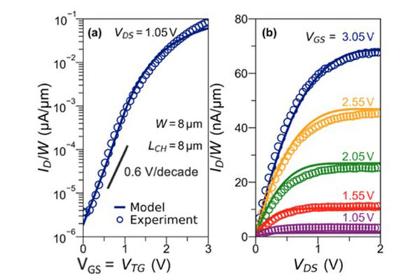
Much of the measurements on atomically thin transistors are obtained from transistors fabricated on specially selected crystals. Once a suitable crystal (with dimensions of approximately 100 square microns) is identified, the transistor and lead arrangements are custom designed to enable fabrication and test. In a paper published in the IEEE Transactions on Electron Devices in April (2020) Mina Asghari Heidarlou shows the results of a batch-fabrication process she developed on materials grown by Bhakti Jariwala at Penn State by chemical vapor deposition. Her study of approximately 100 transistors gives a first look at two-dimensional materials in processes that are translatable to manufacturing. Paolo Paletti shows that the characteristics are well described by a simple compact model.